Applied Materials strives to cooperate with
chipmakers to shorten equipment lead time
By Nam Hyun-woo, The Korea Times - Applied
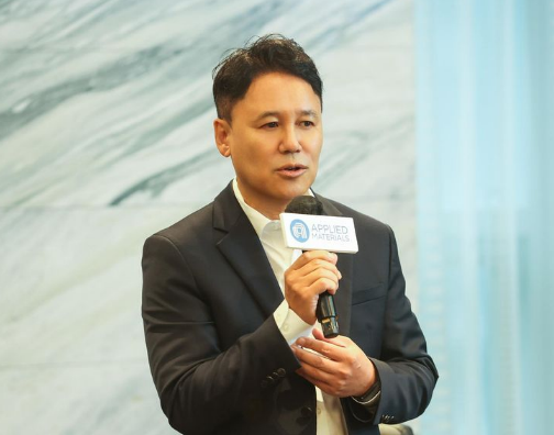
Materials Korea Country President Park Gwang-sun said Monday that the
semiconductor engineering solutions company is working to help Korean
chipmakers optimize performance and maximize output as they expand globally.
During a press conference in Seoul, Park
said Korea’s strategic importance in the global artificial intelligence (AI)
ecosystem has been reassessed in the past year, adding that one of the
company’s most important roles is to work closely with customers to forecast
long-term demand and supply equipment accordingly.
“We are working closely with our
customers to optimize design and maximize output so that our equipment can
produce high-quality devices,” Park said.
“Our customers have recently been
expanding their fabs globally. SK hynix announced its Indiana fab last week,
while Samsung has already begun operations at its Taylor fab. As they expand
their global footprint, Applied Materials Korea is working to ensure seamless
technical and workforce support.”
The comments came as demand for memory
chips continues to far outpace supply, prompting chipmakers to expand capacity
and place additional orders for Applied Materials equipment.
“Our ability to respond to equipment
demand is limited in the short term, but we will be much better positioned to
meet demand two to three years from now,” Park said. “We are discussing with
our customers how to prepare for at least the next three years, rather than
focusing on issues over the next three or six months.”
During the conference, Applied Materials
Vice President Mukund Srinivasan said the semiconductor industry faces two key
challenges: technology and capacity.
On the technology side, he said
addressing the memory wall, where memory performance fails to keep pace with
logic chips, requires 3D scaling in logic and memory chip manufacturing and
packaging.
According to Srinivasan, 3D scaling is
an architectural approach that encompasses technologies that stack or integrate
components vertically to shorten the physical distance that data must travel
and improve energy efficiency. Examples include Gate-All-Around technology for
logic chips, stacking memory die in high-bandwidth memory and hybrid bonding
for packaging.
“So I would say 3D scaling is how the
technology problem is being solved,” he said. “The entire ecosystem has to ramp
up, starting with our customers who are building fabs to make enough logic and
memory, and then coming to us to supply the machines. … So the industry is
working together from a total ecosystem perspective.”
To achieve this, he said Applied
Materials is expanding its Equipment and Process Innovation and
Commercialization (EPIC) Center program, in which customers, partners,
universities and research institutions collaborate from earlier stages of
development to reduce the gap between technology research and mass production.
Samsung Electronics and SK hynix are
founding partners of the EPIC Center, and the number of collaborative projects
under the program has expanded to 11. While the EPIC Center in Silicon Valley
focuses on innovation and commercialization, the Applied Collaboration Center
Korea in Osan, Gyeonggi Province, supports technology development and
validation for mass production.
Source: https://www.koreatimes.co.kr/business/tech-science/20260831/applied-materials-strives-to-cooperate-with-chipmakers-to-shorten-equipment-lead-time