SK hynix confirms new packaging fab construction in
Cheongju
Political pressure builds over where to place chip
investment
By Nam Hyun-woo, The Korea Times - SK hynix on Tuesday
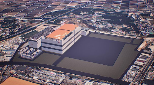
confirmed the construction of its new semiconductor packaging fab, dubbed
P&T7, in Cheongju, North Chungcheong Province, as the memory giant
accelerates expansion of its production capacity for high-bandwidth memory
(HBM) for artificial intelligence (AI) accelerators.
On its website, SK hynix said it will invest 19 trillion
won ($12.92 billion) to build the P&T7 fab on a 230,000-square-meter site
in the city’s industrial complex. Construction is set to begin in April with
completion targeted for the end of 2027.
The company said it is “a strategic decision that reflected
the government’s policy goal of balanced national growth while also taking into
account supply chain efficiency and future competitiveness.”
According to the company, P&T stands for packaging and
testing, and P&T7 will be an advanced packaging facility that turns chips
produced at front-end fabs into finished products and conducts final quality
inspections.
The P&T7 plan has been rumored since June 2025, as the
company demolished buildings on the site of LG’s former Cheongju Plant 2 that
SK hynix had previously acquired to make way for a new packaging facility.
P&T7 is designed to work in tandem with the existing
M15 fab and the M15X facility now being built for HBM production in Cheongju.
Of the two, SK hynix invested 20 trillion won in M15X, which opened its
cleanroom in October 2025 ahead of schedule and is now in the final stages of
equipment installation.
Along with M15 and M15X, SK hynix has M11, M12 and P&T3
fabs in Cheongju, which is about 130 kilometers south of Seoul.
"The
organic link between the M15X and P&T7 is expected to position the city as
SK hynix’s new core hub for AI memory, as well as strengthening its ability to
meet rising demand for advanced memories,” SK hynix said.
While announcing the new investment, SK hynix stressed the
decision aligns with the government’s policy goal of balanced national growth.
"Amid
the rapid shifts in the investment environment surrounding the semiconductor
industry, there are debates over the meaning and role of investments in the
noncapital area,” the company said.
"SK
hynix sees beyond short-term efficiency or immediate gains, and seeks to make
contribution in strengthening the country’s industrial foundation over the long
term and building a structure in which the capital and noncapital regions grow
together.”
The company referred to debates among political voices that
semiconductor fabs should be located across the country for balanced growth
alongside the semiconductor industry’s hesitation, citing infrastructure and
workforce issues.
President Lee Jae Myung on Dec. 10, 2025, told Samsung
Electronics’ chip division head Vice Chairman Jun Young-hyun and SK hynix CEO
Kwak Noh-jung that he hopes for “semiconductor companies to turn their eyes to
the southern region and make contributions to the country’s balanced
development.” Minister of Climate, Energy and Environment Kim Sung-hwan also
floated the necessity of dispersing the chip cluster during a radio interview.
The comments were interpreted to be targeting that
semiconductor complex that the two companies are building or set to build in
Yongin, Gyeonggi Province, about 50 kilometers south of Seoul. SK hynix had
already begun construction, while Samsung Electronics has recently signed deals
to purchase land in Yongin.
Lawmakers from the southern part of the country have also
raised their voices, with those from North Jeolla Province urging the
industrial complex to be relocated to the province’s Saemangeum area, about 250
kilometers southwest of Seoul.
Though presidential spokesperson Kim Nam-joon said Thursday
that any relocation decision would be up to the company, lawmakers’ calls are
growing. Semiconductor industry officials expressed concern that political
considerations could end up dictating corporate decisions based on feasibility,
because both Samsung and SK hynix considered Yongin’s grid infrastructure,
water resources and the advantage of the capital area in attracting workers.
Samsung Electronics operates its main semiconductor
complexes in Yongin, Hwaseong and Pyeongtaek, all in Gyeonggi Province, which
surrounds Seoul. It also has a packaging facility in Asan, South Chungcheong
Province, located about 100 kilometers south of Seoul.
Source: https://www.koreatimes.co.kr/business/tech-science/20260113/sk-hynix-confirms-new-packaging-fab-construction-in-cheongju


